In the sensor device process, firstly,electric circuits (patterns)
are formed on wafer front surface. Secondly, backside of wafer is
grinded for thinning. Wafer with device patterns are very valuable
to customers and they need to be handled with care. Rokko’s process
is able to treat wafers without damaging patterns with severely
selected protection tapes. Similar to the power device grinding
services, a special grinding wheel that stimulates growth of a gettering
layer on processing surface is also available.
Rokko’s strength lies in the well-developed sensor device process
technologies that enable the company to provide integrated grinding
and polishing services.
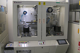
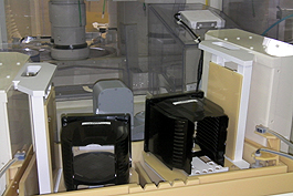
■ Tools and Equipment
Wafer protection tape
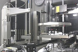
applicator
Fully automated grinding
machine
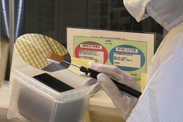
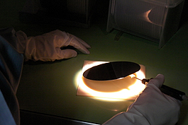
After incoming inspection, pressure sensor or UV tapes are
applied on wafers. Taped wafers are inspected of adhered dusts
during this process.
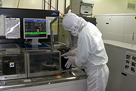
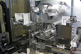
Capable of polishing wafers of 4 to 8 inch without influencing
flatness characteristics.
Visual inspection
Single wafer system polishing
machine
Wafer appearance is checked in this process.
Polishes wafers to meet customer’s thickness specification.
Non-contact type processing
surface tape remover
Ultrasonic cleaning tool
Remove tapes without contacting processed surface.
Cleans wafers by ultrasonic after removal of tapes.
Final inspection
Wafers are inspected based on customer’s visual inspection
criteria.
● Automatic spectral interference
wafer thickness meter
Thickness can be measured for the silicon layer only of the
taped wafer・SOI・supported wafer・resin-material/tape supported
wafer(in case 2 silicon wafers are attached, one side silicon
layer can be measured).
● Automatic spectral interference
wafer thickness meter
Thickness can be measured for supporting silicon layer only
or active layer only, other than the total thickness measurement
of wafer, for the thinned MEMS/Sensor wafer.