『Meeting customer expectations』
● How do you prevent wafers from being broken
or chipped after wafer thing process? These damages are mainly caused
by either human handling or equipment conveyance and it dose affects
your process yield. How do you want to solve this problem?
『Customer needs』
● How do you remove stains on patterned
or filmed wafer’s surface after thinning / polishing process?
● Do you have any wafers that you cannot input into your process
because of the cleaning capability of your equipment?
※In the conventional cleaning process of
polished back surfaces, organic or DI wafer based techniques are
used to clean particles. In order to remove metal contaminations
from the surfaces, it requires RCA cleaning but this method cannot
be used because normally RCA cleaning will etches and damages
surface of patterns or films.
To meet such customer needs in the semiconductor backend process,
Rokko has developed “Rokko Premium Process” through the collaboration
with equipment manufacturers.
■ Process
Conventional
process
Protective
taping
Backside
grinding
Single
wafer
Backside polishing
Processed
surface
contactless tape
peeling
Rokko
Premium
process
Protective
taping
Knife
edge
preventive process
Backside
grinding
Single
wafer
Backside polishing
Processed
surface
contactless tape
peeling
RCA
cleaning
process for
patterned wafer
■ Knife
Edge preventive process
『Customer needs』
● How do you prevent wafers from being broken
or chipped after wafer thing process? These damages are mainly caused
by either human handling or equipment conveyance and it dose affects
your process yield. How do you want to solve this problem?
→
Rokko provides pre-grinding beveling services meeting the diversified
requirements of finished thickness (ex. 100 um or 50um).
Through the NC control beveling, Rokko is capable of processing
wafers with various thickness without changing polishing pads.
Before BG
Beveling
After BG
※Non-beveling process
※Forming a knife edged shape
※Beveling process
※Beveling compatible with various
wafer thickness to form a proper edge profile
Crick here for the video clip showing a dropping test result
of 6 inch wafers “with” and “without beveling” →
● Knife edge preventing process
unit
Wafer size: 4, 5, 6, 8 Inch
● Knife edge preventing process
unit
Through NC control system, shapes of edge can be adjusted
according to its thickness.
■ Back
Grinding
Rokko has over 10 years of experiences in the wafer thinning business
with various types of wafers from SOI・glass/Si mounted to normal
mass production wafers (100-150um thickness).
We are making our continuous efforts to improve the yields of wafers
received from our customers.
MEMS applications: SOI・glass/Si mounted, through-holed, cavity structured,
through-silicon via (TSV) and non-circular wafers
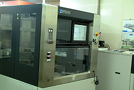
● Backside Grinder
Wafer Size: 4, 5, 6, 8 Inch
● Backside Grinder
Achieving higher yields through daily maintenance checks.
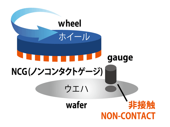
■ New Functions: In the conventional process, wafer thickness is measured
by an in-process gauge. Rokko has just installed the machine equipped
with NCG (non-contact type gauge) which allows the machine to measure
wafer thickness by laser without touching. In the newly developed
process, all wafers including MEMS such as cavity structured, holed
wafers can be measured. ■Wafer Size:5・6・8inch
■Thickness: 100~150μm
■MEMS Wafer process
Rokko is well experienced in processing various kinds of wafers
such as SOI・glass/Si mounted, through-holed, cavity structured,
through-silicon via (TSV) and non-circular wafers.
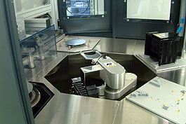
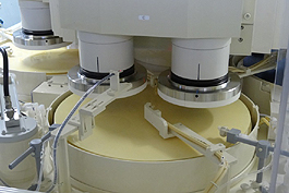
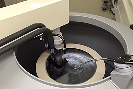
■ Single
wafer backside polishing
In this process, wafers are mirror-polished by removing small roughness
on a wafer surface. This process requires highly sophisticated polishing
techniques to avoid any distortions or scratches on wafer surfaces.
■Merits of Single wafer process:
●It is a wax-less process that allows to achieve higher cleanness
levels by reducing cleaning requirements.
●A single wafer process equipment can polish wafers more efficiently
than the batch type and it also requires less removals in comparison.
●A single wafer process provides more accurate polishing and it
also helps to achieve higher flatness levels.
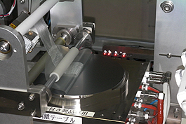
● Single wafer backside polishing
equipment
Wafer Size: 4, 5, 6, 8 Inch
● Single wafer backside polishing
equipment
This machine is capable of processing thinned wafers and MEMS
wafers.
■ New equipment:8
inch single wafer polishing machine ■Wafer Size:4・5・6・8inch
■Best thinning achievement:8inch 85μm
● Backside polishing equipment
for 8-inch
Wafer Size:4・5・6・8inch
● Backside polishing equipment
for 8-inch
Best thinning achievement:8inch 85μm
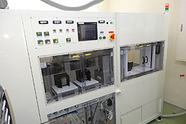
■ Automatic
scrub cleaning process
■ New Equipment:
After polishing, residues contain alkaline substances results in
becoming polishing marks or sources of particle. Removing such residues
before coated by native oxide films is one of the key techniques
in polishing.
In our conventional process, wafers are cleaned piece by piece through
operator’s manual scrubbing. Now, Rokko introduced the automated
cleaning equipment to eliminate human errors and deviation of quality
to achieve the uniform stable quality.
■Wafer Size:4・5・6・8 inch
■Thickness: ~ 100μm
■Patterned・ MEMS and SOI Wafer
Glass supported wafers also can be processed.
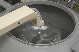
● Automatic scrub cleaning process
High cleaning performance.
● Automatic scrub cleaning process
Wafer Size:4・5・6・8 inch
Sapphire and SiC wafers can be processed
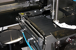
■ Processed
surface contactless tape peeling
Protective tapes are peeled off from wafers without touching processed
surfaces.
■Wafer Size: 5, 6 Inch
■Tape Type:UV tapes
■Characteristics:
●By Bernoulli chucking robotic arms, wafers are conveyed without
being touched.
●After wafers are set on the stage for UV irradiation process, through
this procedure, protective tapes on wafers are removed automatically.
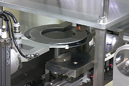
● Processed surface contactless
tape peeling unit
Wafer Size: 5, 6 Inch
● Processed surface contactless
tape peeling unit
Post-polishing surfaces are very fragile. Micro-scratches
can be caused easily if the surface is touched by any metallic
equipment parts. This unit is capable of removing tapes without
touching wafer surfaces.
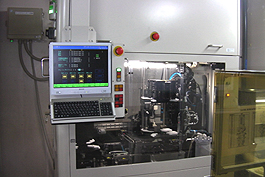
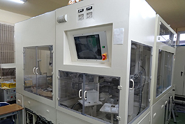
■ RCA
cleaning process for patterned wafers
■Available services
・RCA cleaning for wafers with metallic patterns (particle and metal
contamination cleaning)
・RCA cleaning for filmed wafers (particle and metal contaminations
cleaning)
・Wafer backside RCA cleaning for handle wafers or bonded wafers.
(particle and metal contamination cleaning)
■Basic specifications
・Polished surface contactless automated conveyance (cassettes to
cassettes) ・Simultaneous double chambered spinning method (RCA cleaning
⇒DIW rinsing⇒Drying)
・Cleaning metal contaminations by only one chemical treatment.
・4, 5, 6 and 8 inches can be processed with minimum thickness of
150um. (The process for under 150um is under development.)
・Handle wafers can be processed in Rokko.
■Cleanness (Patterned wafer backside)
Particles: ≧0.3um,≦50pcs/wf
Heavy metals:≦5.0E10atoms/㎝-2
(Ka,Ca,Ti,Cr,Mn,Fe,Co,Ni,Cu,Zn,Al,Na)
Click here for a demonstration of wafer backside RCA cleaning
of patterned wafers→
● RCA cleaning process for patterned
wafers
Wafer Size: 4, 5, 6, 8 Inch
● RCA cleaning process for patterned
wafers
This equipment is capable of cleaning only onside (backside)
without causing any damages on the other side.