Rokko is making continuous efforts to develop new technologies
in not only Si wafer but also sapphire and SiC process through
our cultivated experiences in grinding, polishing and cleaning
fields. We believe customer satisfaction is the base of our technology
development and our success cannt be achieved without the support
from our customers. Based on this standard, we will make further
efforts to ensure the satisfaction by introducing cutting edge
equipment and technologies.
● Automatic spectral interference
wafer thickness meter
Thickness can be measured for the silicon layer only of the
taped wafer・SOI・supported wafer・resin-material/tape supported
wafer(in case 2 silicon wafers are attached, one side silicon
layer can be measured).
● Automatic spectral interference
wafer thickness meter
Thickness can be measured for supporting silicon layer only
or active layer only, other than the total thickness measurement
of wafer, for the thinned MEMS/Sensor wafer.
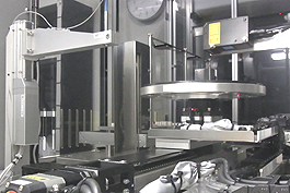
■ New equipment:Wafer
sorter for resistivity・P/N・thickness
● Wafer sorter for resistivity・P/N・thickness
For 4,5,6,8 inch
● Wafer sorter for resistivity・P/N・thickness
Measurable resistivity:1.0m~3.0MΩ・cm
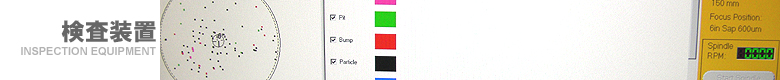
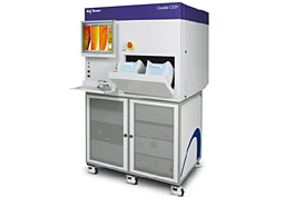
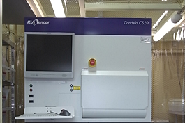
Candela CS20 Wafer surface
inspection machine
Candela CS20 Wafer surface
inspection machine
This is used for transparent substrates to inspect various
defects, dirt, pits on Epi layers, hatching and crystal damages.
Wafer Size: 3, 4, 5, and 6 Inch
Measurable thickness: 300-1400um
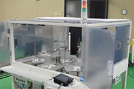
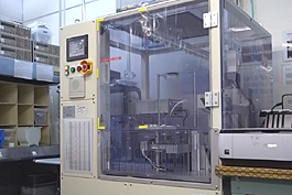
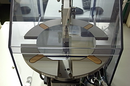
This equipment unloads wafers from cassettes and measures
thickness at a designated coordinate of wafer. The measurement
is done by a contactless capacitance sensor.
Measurable thickness: 100-1800um (depends on wafer sizes)
Center point measurement (Coordinates can be set through the
machine configuration)
Total reflection x-ray
fluorescence analysis tool TREX610
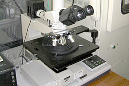
Differential interference
contrast microscope
Measurable elements: 12 elements (S, Cl, K, Ca, Ti, Cr,Mn,Fe,Co,Ni,Cu,Zn)
This tool allows to observe roughness on a wafer surface.
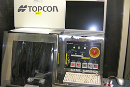
Wafer surface laser inspection
tool TOPCON WM7
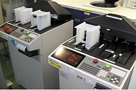
Wafer surface laser inspection
tool TOPCON WM3
Detection limit: 7um
Unit: Long-life Violet LD laser type
Wafer Size: 4, 5 and 6 Inch
Ranges:0.087μ~5.0μ
Wafer Size: 4, 5 and 6 Inch
Rages:0.208μ~1.0μ
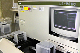
Wafer surface laser inspection
tool LS6030
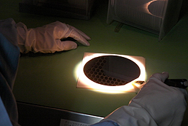
Visual inspection
Wafer Size: 5, 6, 8 Inch
Ranges:0.1μ~5.0μ
Wafers are inspected under a halogen lamp in a dark room.