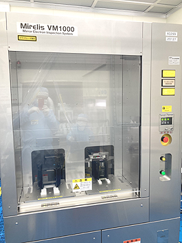
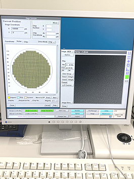
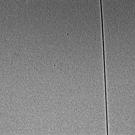
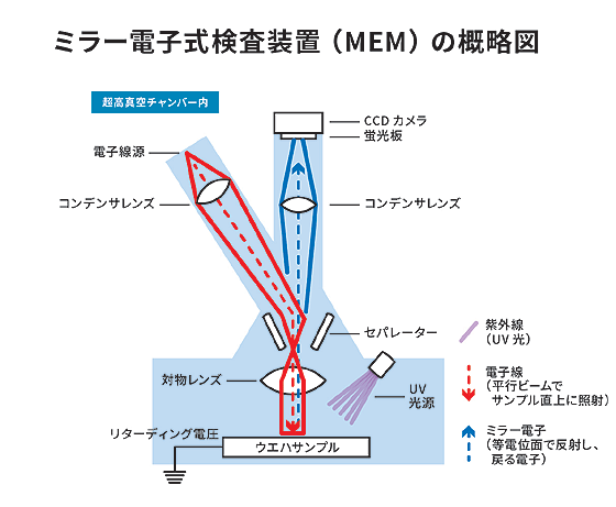
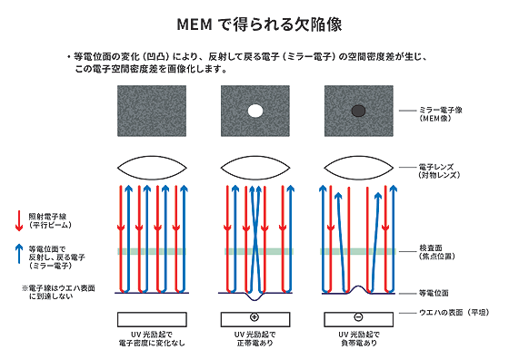
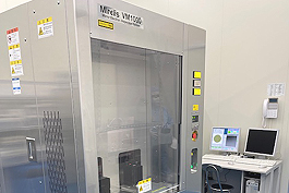
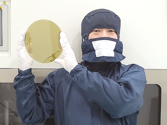
● Mirelis electron microscope
【MEM】
※8-inch SiC measurement available
※Contract inspection services available.
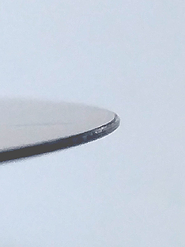
Used as a surface (Si surface) latent flaw inspection machine
to check for processing damage and defects.
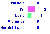
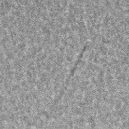
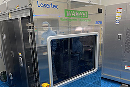
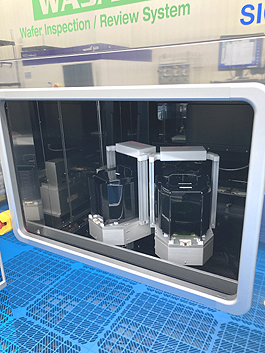
● SiC wafer defect inspection
and review system 【SICA88】
※8-inch SiC measurement available
※Contract inspection services available.
Used for scratch inspection of surfaces (Si side and C side),
and for checking pits, defects, etc.
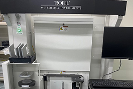
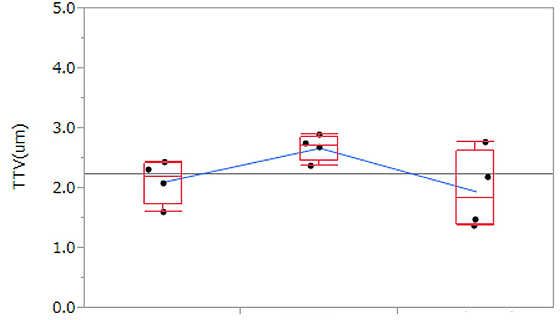
● Wafer flatness measurement
and analysis system
【Tropel】
※Contract inspection services available.
Used to check flatness before and after processing.
TTV, NTV, SORI, BOW, WARP, etc.
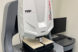
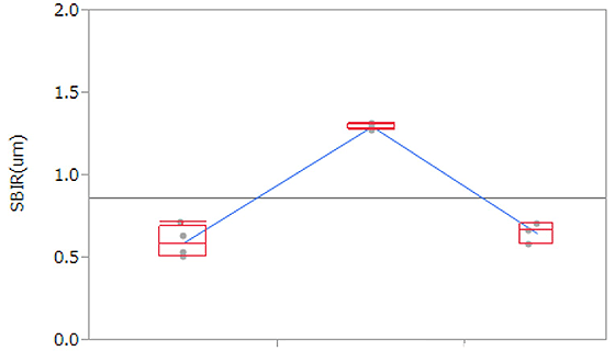
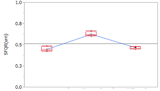
● Surface roughness measuring
instrument 【Zygo】
※Contract inspection services available.
Used for checking surface roughness after machining (non-contact
measurement).
Roughness measurement after grinding and CMP (Chemical Modulation).
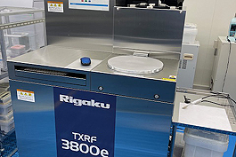
● Total Internal Reflection X-ray
Fluorescence Analyzer 【TXRF】
※Contract inspection services available.
Metal contamination and full-surface sweep measurement possible《[S
Cl K Ca Ti Cr Mn Fe Co Ni Cu Zn》
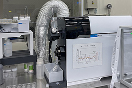
● Inductively coupled plasma
mass spectrometer
【ICP-MS】
※Contract inspection services available.
Metal contamination and various metals can be measured


.gif)