Grinding and polishing are the core technologies that decide the
quality and the characteristics of semiconductors. Rokko is continuously
developing its process by adopting new technologies created by consecutive
improvements. Because of this effort, Rokko takes a very important
role in the fields of MEMS special wafer grinding and polishing
processes and its highly established technologies enable the company
to fulfill customer’s requests derived from various phases such
as R&D or volume productions.
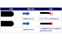
Due to the thinness of the finished wafer,
the bevel shape of the wafer before processing becomes sharp
like a knife, which can cause chipping. We can perform processing
to prevent this beforehand.
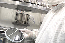
Precise grinding is the very important factor
for eliminating thickness deviations. In this process, the
right type of machine that meets customer’s requirements is
carefully selected among the variety of process equipment.
Rokko’s grinding technologies are able to guarantee the minimum
thickness of 15um in prototyping and 100 to 150um in volume
productions.
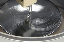
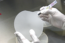
After grinding, small roughness is created
on wafer surface. In this process, wafers are carefully polished
to remove the roughness. The polishing needs to be done in
precise and speedy manners to avoid any distortions and scratches
on wafer surface.
Rokkos’s technologies enable the company to
provide integrated grinding and polishing services for MEMS
(Micro Electronics Mechanical System) processed wafers such
as SOI・glass/Si mounted, through-holed, cavity structured,
through-silicon via (TSV) and non-circular.
For parts with a pattern on the front, the
back side is thinned, and when returning them to the customer's
process, only the thinned surface is RCA cleaned to remove
metal contaminants and then returned. (The RCA cleaning will
not reach the patterned surface.)
There is a need to process silicon and compound
wafers to a thickness of ≤100um, but there are limitations
to using a single wafer, such as moving a thinned wafer to
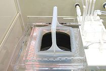
the next process. For such wafers, a support substrate is
used to continuously support them until the dicing process
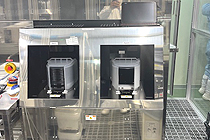
The introduction of a double-sided polishing
machine has enabled us to achieve in-plane TTV < 1 μm.
This allows us to handle the processing of silicon for bonding
substrate materials.
We perform refinishing and polishing of monitor
wafers required for each stage of your process. We will provide
services tailored to your needs, including thickness control,
particle control, and metal contamination control. We can
handle wafer sizes from 4 to 8 inches.
For ultra-flattening processes that cannot
be achieved through grinding and CMP machining, we use trimming
as a final finishing step to achieve nanometer-level flattening.
We also offer a service to remove contaminants
from monitor wafers by etching away the various films and
then performing RCA cleaning. We can also verify that all
contaminants have been completely removed through various
inspections. If particle-free guarantees are required, we
can accommodate this through our standard reprocessing service.
In our support service, we mount the thinned
wafers, which have gone through your heating and chemical
processes, onto a dicing ring, remove the support material,
and return them to you.