Rokko has the established sophisticate polishing and grinding technique
to process front/back surface with high accuracy through its integrated
process in order to deliver the finished products to time to meet
customer’s needs. This experience allows the company to meet diverse
demands of grinding and polishing required by MEMS or other related
applications. Rokko always appreciates any inquiries and orders
of any size.
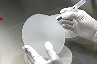
■ Processing services
●
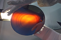
Integrated processing of beveling, grinding, polishing,
and cleaning
We process and manage wafers to achieve the thinness
and mirror finish required for sensors and power devices,
using a consistent process of beveling, grinding, polishing,
and cleaning. We can handle wafer sizes from 4 to 8
inches, and polished finish thickness (prototype-mass
production) ≤ 100um. In addition to this consistent
process, we also accommodate diverse requirements such
as grinder finishing (Ra: 2-3nm) and polishing only.
●
Monitor wafer reclaiming services
We perform refinishing and polishing of monitor wafers
required for each stage of your process. We will provide
services tailored to your needs, including thickness
control, particle control, and metal contamination control.
We can handle wafer sizes from 4 to 8 inches.
●
MEMS Process
Rokko’s experience in this field enables to meet the
diverse needs in MEMS applications through its special
grinding and polishing technique. This service can be
applied from a single wafer production to large volume
or prototyping to mass productions. Rokko is well experienced
in grinding and polishing SOI・glass/Si mounted, through-holed,
cavity structured, through-silicon via (TSV) and non-circular
wafers.
There is a need to process silicon and compound wafers
to a thickness of ≤100um, but there are limitations
to using a single wafer, such as moving a thinned wafer
to the next process. For such wafers, a support substrate
is used to continuously support them until the dicing
process.
Amidst the diverse needs of various devices, there are
cases where ultra-thinning and ultra-planarization of
substrates are required. To meet these needs, our company
has achieved ultra-thinning and ultra-planarization
of substrates (controlling in-plane TTV at the nm level).
We can also perform oxide film planarization.
We can handle various types of compound wafers, processing,
and inspections. ⇒ Please refer to the
compound wafer page for details.
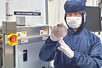
■ Process Quality
All services are performed under the clean
controlled environment. Rokko is obtained Environment Management
System (ISO14000) and Quality Management System (ISO9001)
certifications to comply with the international standards/
●
Pursuit of Quality
Quality is the 1st priority in Rokko’s operations. All
parameters are measured and monitored, which includes
thickness accuracy, polishing precision to give customers
the best available quality and services.