Rokko takes the following roles in the semiconductor production
process.
- Wafer surface and backside sophisticate grinding and polishing
- Monitor wafer reclaiming
- Chemical processing and RCA cleaning to control metal contaminations
and particles in reclaim wafer process.
- Special wafer processing for MEMS applications
■ Inspection correspondence
table by material
○-Mark = Inspection available Each material * Each inspection
details
Material
Face
Particles
Contamination
Flatness
Thickness
ICP-MS
TXRF
Zygo
TTV
SBIR
SFQR
BOW
Warp
SORI
contact type
non-contact type
Resistance
P/N
MEM
SICA
Silicon
○
○
○
○
○
○
○
○
○
○
○
○
○
○
○
N-dope SiC
Si-face
○
○
○
○
○
○
○
○
○
○
○
○
○
C-face
○
○
○
○
○
○
○
○
○
○
○
○
○
Semi-insulating
SiC
Si-face
○
○
○
○
○
○
○
○
○
○
○
○
C-face
○
○
○
○
○
○
○
○
○
○
○
○
SiC Epi wafer
○
○
○
○
○
○
○
○
○
○
○
○
○
Polycrystalline
SiC
○
○
○
○
○
○
○
○
○
○
○
○
LiTaO 3
○
○
○
○
○
○
○
○
○
○
○
LiNbO3
○
○
○
○
○
○
○
○
○
○
○
GaN
Ga-face
○
○
○
○
○
○
○
○
○
○
○
N-face
○
○
○
○
○
○
○
○
○
○
○
Sapphire
C-face
○
○
○
○
○
○
○
○
○
○
○
R-face
○
○
○
○
○
○
○
○
○
○
○
Ga2O3
○
○
○
○
○
○
○
○
○
○
○
AlN
Al-face
○
○
○
○
○
○
○
○
○
○
○
N-face
○
○
○
○
○
○
○
○
○
○
○
Quartz
○
○
○
○
○
○
○
○
○
○
○
○
GaN on Si
○
○
○
○
○
○
○
○
○
○
○
○
GaN on Sap
○
○
○
○
○
○
○
○
○
○
○
○
GaN on SiC
○
○
○
○
○
○
○
○
○
○
○
○
SOI
○
○
○
○
○
○
○
○
○
○
○
○
○
Oxide film
○
○
○
○
○
○
○
○
○
○
○
○
○
○
Glass
○
○
○
○
○
○
○
○
○
○
○
○
■ Processing compatibility
chart by material
○-Mark = Processable Each material*Each processing content
■Tape bonding compatible with 4,
6, and 8-inch wafers. ■Resin bonding compatible with 6 and
8-inch wafers. Resin bonding is also possible for wafers with
resist.
■ Support substrates are available.
■Terrace processing is available.
■4-8 inch
■Bumped wafer
■Pressure sensor mounted or UV taped wafer
■Ring-framed wafers
■4-8 inch compatible
■ Backside thinning
■ Si-side and C-side epitaxial regeneration processing
■ Film removal etching
■ Wafer making
■ Various measurement services
■4-8 inch compatible
■ Various wafer processing services
■ Beveling, grinding, polishing, cleaning, support, etching,
etc.
■ Various measurement services
■4-8 inch compatible
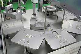
■SICA88
■MEM
■TROPEL
■ZYGO
■TREX
■ICP-MS
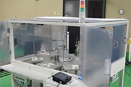
■ Introduction and description of the used equipment in each
process
UV irradiator
Fully Automated Grinding
machine
Remove the UV tape (Also includes a dicing ring)
Capable of a single wafer and multiple wafer productions.
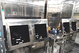
Dual steam cleaning tool
This single tool provides DIW cleaning, rinsing and air drying
to wafers up to 8 inch diameter.
8-inch wafers can also be reclaimed.
Monitor wafer reclaiming
This is recycling services
enables monitor wafers used in the semiconductor process to
be used again by refining their conditions to the original
quality.
Through the services, monitor wafers can be used repeatedly
to reduce material costs.
Wafer size:
3 inch
4 inch
5 inch
6 inch
8 inch
Film
stripping
Selected recipe
Incoming
inspection
Polishing
Classify thickness and film type
Shipping
Final
inspection
Cleaning
Particle,Metal contamination,Thickness
RCA cleaning
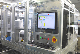
■ New equipment:Wafer
sorter for resistivity・P/N・thickness
● Wafer sorter for resistivity・P/N・thickness
For 4,5,6,8 inch
● Wafer sorter for resistivity・P/N・thickness
Measurable resistivity:1.0m~3.0MΩ・cm
■ Tools and Equipment
Film sorting
Film stripping
Wafers are sorted by different types of films by well experienced
operators.
Films on wafers are removed by the selected chemicals.
Thickness sorting
Batch system polishing
machine
Wafers are sorted by thickness after film stripping.
Multiple wafers are polished concurrently.
RCA cleaning
Particle counter
Wafers are cleaned to remove metal contaminations and particles.
We inspect the particles in the polished wafer.
Flatness measuring device
Final inspection
We will measure the BOW, WARP, and TTV of the polished wafer
Wafers are inspected to comply with customer’s specifications.
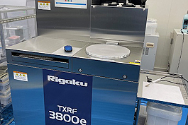
Total Internal Reflection
X-ray Fluorescence Analyzer 【TXRF】
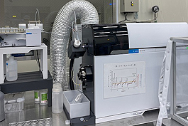
Inductively coupled plasma
mass spectrometer
【ICP-MS】
※Contract inspection services available.
Metal contamination and full-surface sweep measurement possible《[S
Cl K Ca Ti Cr Mn Fe Co Ni Cu Zn》
※Contract inspection services available.
Metal contamination and various metals can be measured